What's new—June 2026
This update was published in June 2026 and includes several enhancements listed on this page.
Visualizing wire bonds
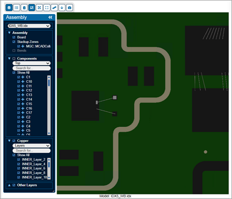
You can now view wire bond data from baseline IDX version 5 files or by uploading an external IDX version 5 file. These files are not stored in the database and are not used for collaboration.
The Viewer displays the wire bonds and you can control their visibility using the Other Layers option in the Assembly toolbox. When layer data is available, NX PCB Exchange Connect groups the wire bonds by layer. Otherwise, it displays a single wire bonds group in the toolbox.
Importing simulation data
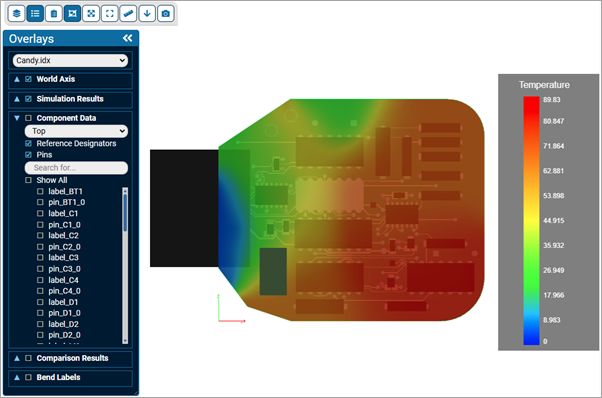
NX PCB Exchange Connect now supports displaying temperature or displacement simulation results on PCB models.
You can upload a spreadsheet or CSV file containing component reference designators and corresponding temperature or displacement values. The Overlays toolbox in the viewer lets you display the imported data as a heat map on the PCB design, to help you easily identify temperature or displacement patterns on the assembly.
IPC-2581C support
NX PCB Exchange Connect now supports importing ECAD models in the IPC-2581C manufacturing format for both rigid and rigid-flex designs, enabling a more complete transfer of PCB data. This helps you exchange PCB data more consistently between ECAD and MCAD environments by importing board geometry, layer definitions, and component data from a single IPC-2581C XML file.
Enhanced net change visualization
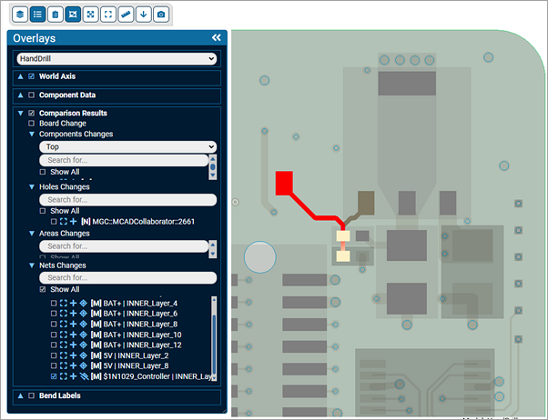
When comparing two PCB designs, the Overlays toolbox in the Viewer now provides additional information and navigation capabilities for comparison results to help you identify and locate net differences more efficiently.
Status letters indicate the type of change: D for deleted entities, M for modified entities, and N for new entities. For net changes, the status letter precedes the net name and layer. For all other PCB entities, the status letter precedes the reference ID. You can view the original reference ID by hovering over an entity to display its tooltip.
You can also isolate and locate selected net changes within the PCB design. When you select a net change, the Viewer zooms to its location, highlights it in a different color, and displays the remainder of the design translucently. After reviewing the change, you can restore the original display.