Exploring the PCB design
Use the Assembly command to explore, visualize, manipulate, and measure the PCB entities in the loaded PCB assembly design.
NX PCB Exchange Connect analyzes the assembly design and displays the assembly information and parameters that describe the board, the components, and other aspects of the assembly in their respective tables arranged in tabs.
You can validate the different milestones of your PCB design cycle by:
- Accessing the PCB entities and their corresponding attributes using interactive tables.
- Visualizing all PCB stack-up layers in a 2D view, either from the top or bottom side.
- Capturing design issues with measurement capabilities.
- Displaying and exploring the PCB entities in the viewer.
- Cross-probing selected entities in the viewer and the tables.
Exploring assembly design workflow
| Steps | Description | Detailed topic |
|---|---|---|
| 1. Load the file. | Load the PCB assembly design from a PCB design file already saved in the database or on the fly. | Loading PCB design files |
| 2. Explore the PCB assembly information and design attributes. | Explore generated information on the board dimensions, layers,
and nets. Visually explore PCB layers types from the top or bottom
side such as:
|
Explore the PCB assembly information and design attributes |
| 3. Filter and search specific entities information. | Filter and search entities information in their respective tabs using interactive tables. | Customize data displayed in the interactive table |
| 4. Graphically explore PCB assembly. | Explore visual representations of the board and its components using the Viewer tab. | Graphically explore drilled holes |
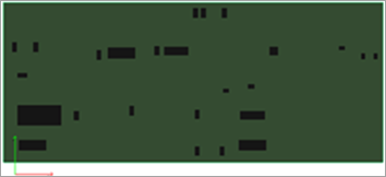
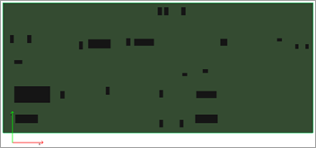
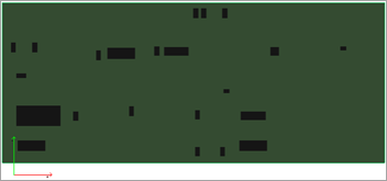
Displaying PCB entities
On the Viewer tab, you can display the entities that you select from the interactive tables.
These tools provide a visual representation of the PCB layout, components, and their interconnections. You can zoom in and out, rotate the view, and inspect individual components and traces in detail.
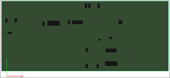
Displaying assembly arrangements
On the Viewer and Components tabs, you can examine various assembly arrangements when design variants are present in the IDX baseline file.
When using the split layout setting on the Components tab, the viewer and interactive table allow you to dynamically examine different arrangements of placed and unplaced components. You can switch between design variants to explore how each arrangement influences the design, and the interactive table automatically filters components to reflect the selected variant. This makes it easy to perform direct comparisons of configuration decisions and evaluate how variant-specific changes affect the end product.
|
|
|
|