Graphically explore drilled holes
This example shows how to graphically explore drilled holes in a PCB design using the 2D viewer.
- On the Assembly loading page, open the desired PCB design.
- On the Assembly main page, click the Drilled Holes tab.
-
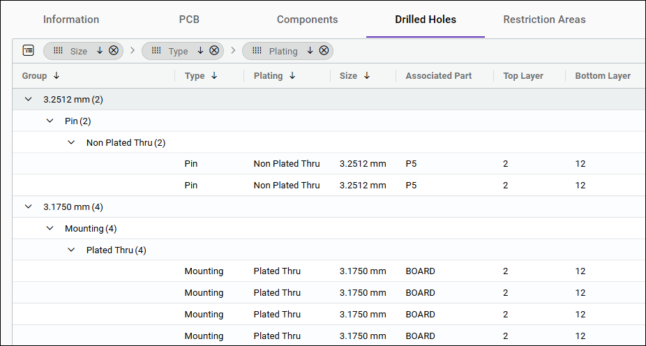
Drag and drop the Size, Type, and
Plating column headings over to the grouping
row.
The table presents the grouped data for drilled holes, categorized by size, type, and plating.
-
To display the full set of data in the grouping, hover over a
Group column heading. Click the column options
 to open quick access commands, and choose
Expand All.
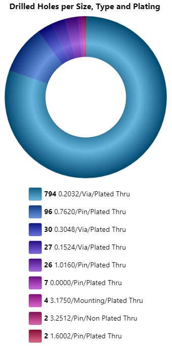
On the right side, the donut chart shows the composition of drilled holes data per size, type and plating. Each segment of the donut represents a specific category, and the size of the segment corresponds to the proportion of that category within the whole set of drilled holes.
You can investigate the segments by hovering over them.
-
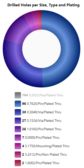
Click on the largest segment in the legend below the donut chart to exclude it
from the visualization and gain insight into the distribution of the remaining
segments.
-
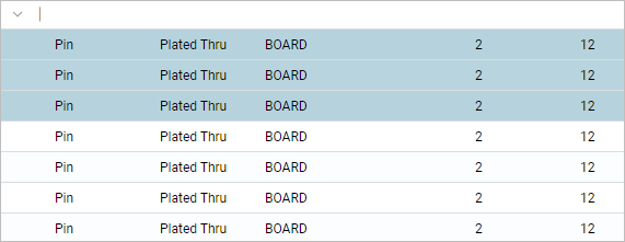
In the table, select the drilled holes by clicking the rows that you want to
graphically inspect.
 Note:When the split layout setting is enabled, the current page displays the content from the Viewer tab directly in the split layout next to the interactive table.
 -
(Optional) When the split layout setting is disabled, to focus on current
selection in the 2D viewer, in the main window, click the
Viewer tab.
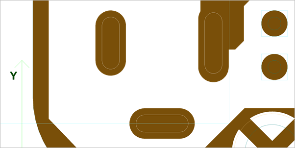
-
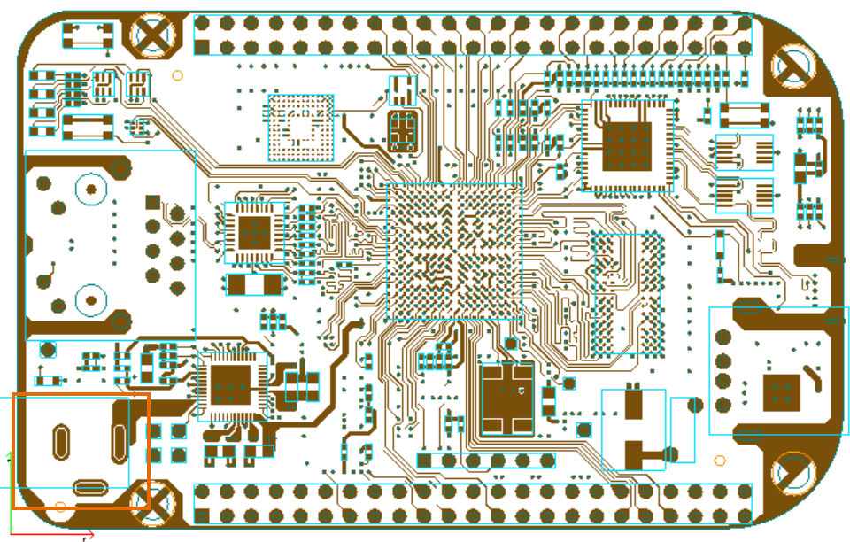
On the viewer command ribbon, click Reset Camera View
 to display the full board.
-
On the viewer command ribbon, click Overlays Toolbox
 .
.
-
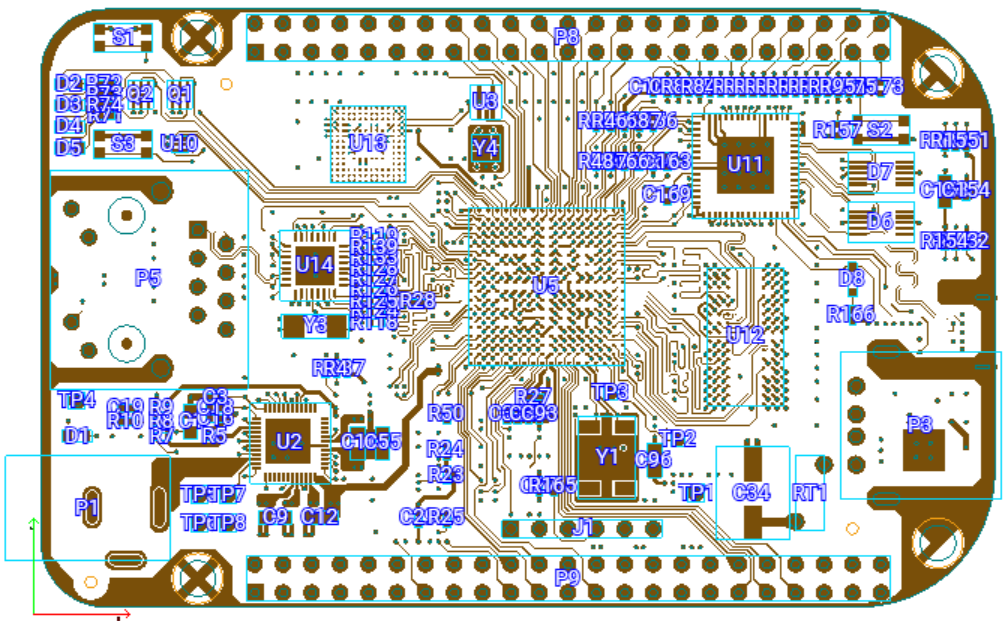
In the Component Data group, select the Show All check box.
The app displays the component labels.
-
On the viewer command ribbon, click Selection Toolbox
 . In
the opened dialog box, the app lists your selection that you select from the
Drilled Holes tabs.
-
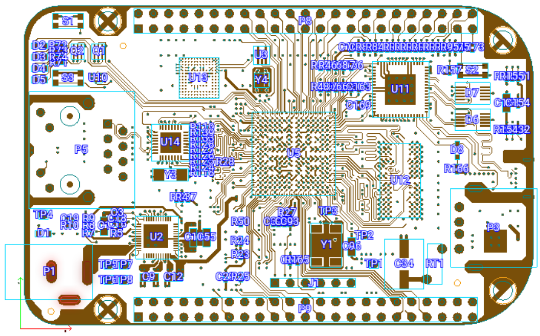
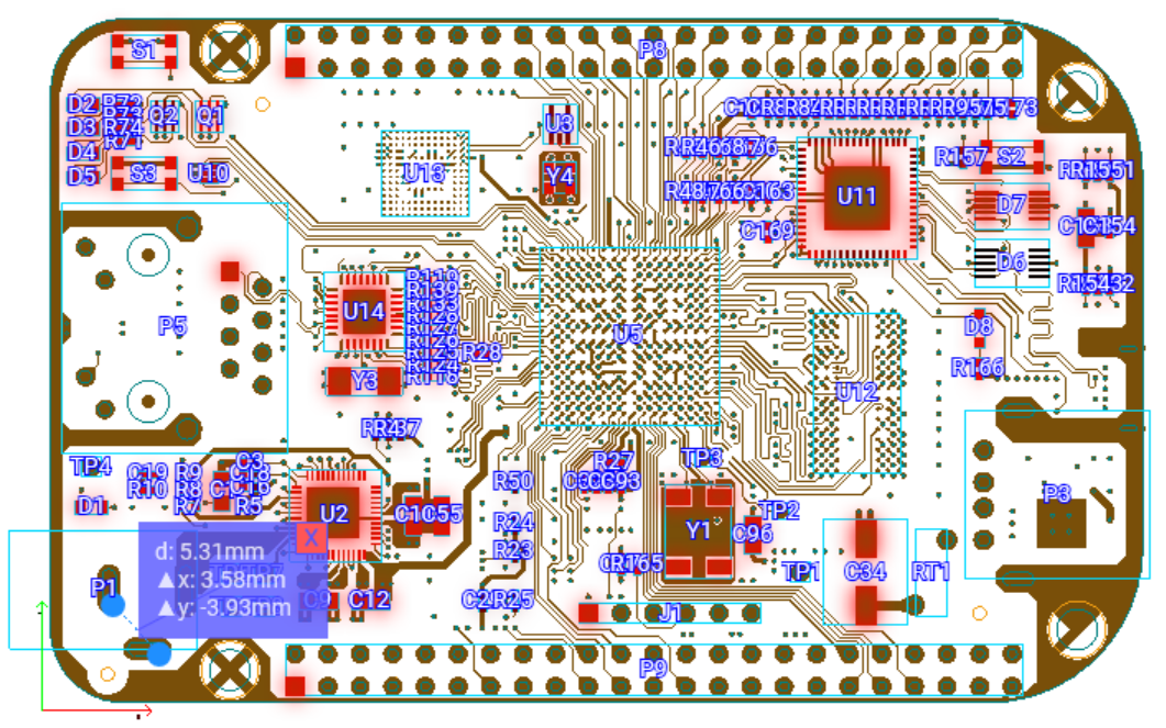
In the Selected Objects group, select all the holes.
The app highlights the holes on the board. You can inspect the placement of these holes, their shapes, sizes, and their connections to any net.
-
On the viewer command ribbon, click Measurement Mode
 to measure
the distance between the holes.
- In the graphics window, select the Snap to Geometry Points check box.
-
Select a point on one hole and another point on the other hole.
The app displays the measurement results in an annotation box.
 .
.
