Compare two PCB designs
This example shows you how to compare two PCB designs using interactive tables and the 2D viewer.
Before following these steps, you need to log in to the web application.
-
Click Compare
 to open the comparison functionality.
If you are not logged in, nothing happens when you click the command.
to open the comparison functionality.
If you are not logged in, nothing happens when you click the command. -
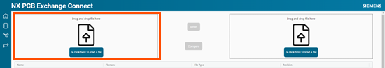
On the top-left corner of the Compare loading page, click
 or drag
and drop the file that contains the first PCB design revision.
or drag
and drop the file that contains the first PCB design revision.
 You can also choose two PCB design revisions from the database table.
 -
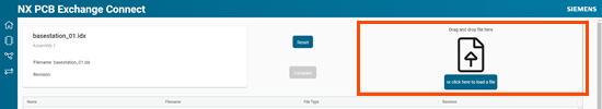
On the top-right corner of the Compare loading page, repeat step 2 to upload a
second PCB design revision.
-
Click Compare to start comparing the two models.
The main Compare page opens with comparison information for the designs and their entities on their respective tabs.
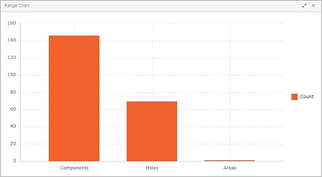
- On the Information tab, in the table, explore the number of PCB assembly changes for each entity type.
-
(Optional) To visualize the chart in different formats, in the Entities
and Count columns, select all the entities and their counts, right-click,
and select your preferred chart format, for example, Chart
Range→Column→Stacked.
-
Click the PCB tab and compare the thickness, sizes,
areas, and layers of the two PCB boards.
When you select a layer in the PCB table, it is highlighted in the corresponding board thickness viewer.
-
On the Components tab, explore the component comparison
table.
The Status column indicates whether the component is unchanged, modified, added or deleted.
-
For modified components, click
 to display more information about the
changes.
to display more information about the
changes.
-
On the Holes tab, explore the holes table.
The Status column indicates if the hole was unchanged, modified, added, or deleted.
-
For modified holes, click to display more information about the
changes.
- On the Area tab, explore the areas comparison interactive table.
-
On the Nets tab, explore the By
Nets and By Layers interactive
tables.
The interactive tables offer different ways to visualize the statuses of nets for each layer of the board.
-
Click the Viewer tab and inspect the graphical display
of the changes between the two revisions.
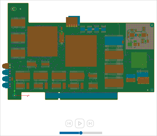 The application displays the added, modified, and deleted components. It also highlights the modified holes using the color code defined in the settings.
 -
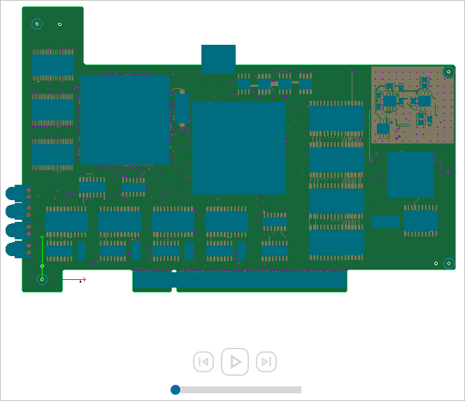
In the graphics window, click rewind
 to display the first PCB design revision.
-
Click play
 to
animate the modification.
to
animate the modification.
-
On the viewer command ribbon, click Overlays Toolbox
 to open the
Overlays toolbox.
In the Comparison Results group, in the Components Changes sub-group, you can display or hide the comparison results of the components mounted on the top, bottom or other layers of the PCB. You can also display or hide any board, hole, area, or net changes from their respective sub-groups.
to open the
Overlays toolbox.
In the Comparison Results group, in the Components Changes sub-group, you can display or hide the comparison results of the components mounted on the top, bottom or other layers of the PCB. You can also display or hide any board, hole, area, or net changes from their respective sub-groups. -
On the viewer command ribbon, click Overlays Toolbox
to close the
Overlays toolbox.
-
In the graphics window, click forward
 to display the
second PCB design revision.
to display the
second PCB design revision.
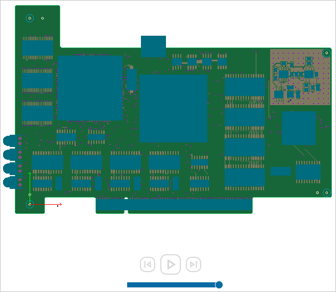 You can use the viewer functionality to explore the design changes in detail.