Cross-select entities
This example shows you how to cross-probe PCB entities between the interactive tables and the viewer.
- On the Compare loading page, open the two PCB designs.
- On the Compare main page, click the Areas tab.
- In the interactive table, click Filters to open the Filters toolbox.
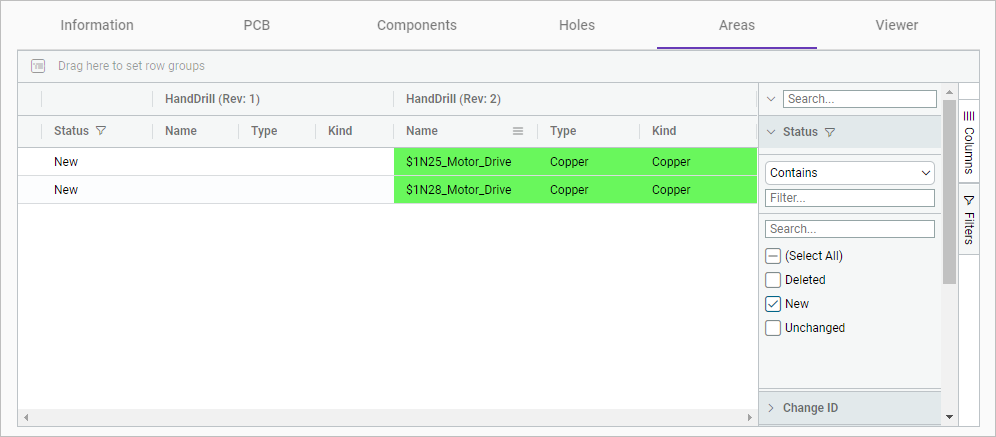
- Expand the Status group and clear the Select All check box to filter the components by status.
-
Select the New check box to display only the new restriction areas in the design.

The PCB design has two new copper areas.
- In the interactive table, select both added areas.
- On the main page, click the Viewer tab to display the 2D layout of the PCB design.
-
On the viewer command ribbon, click Selection Toolbox
 .
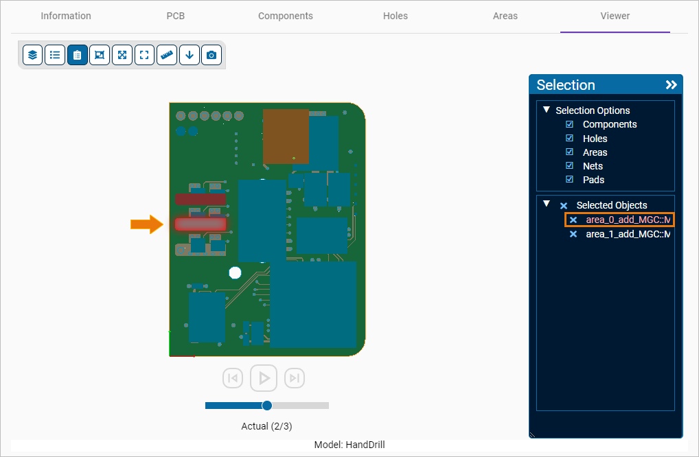
In the Selection toolbox, notice that the PCB entities you selected in the interactive table now display under the Selected Objects list. These objects are displayed in grey on top of the other visible objects in the viewer.
 -
From the Selected Objects list, select any entity to
highlight it on the PCB design.

The application highlights the border of the selected entity on the 2D layout of the PCB design. You can also define a custom color to highlight elements you select on the Settings page.
-
On the viewer command ribbon, click Overlays Toolbox
 .
.
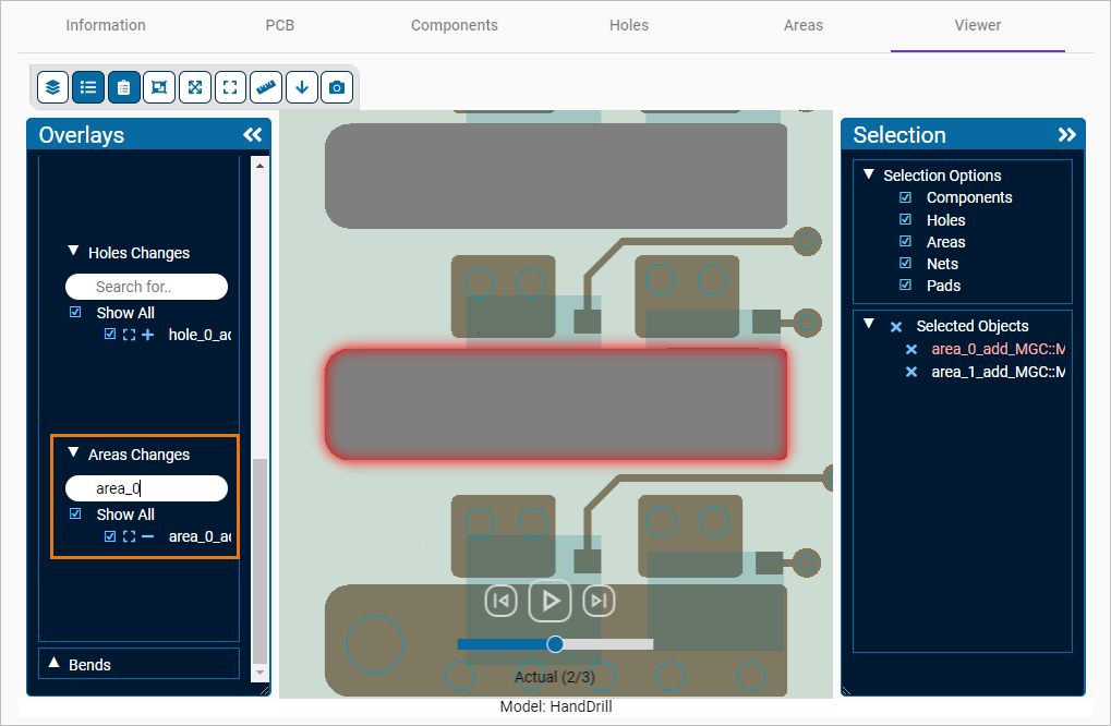
- In the Overlays toolbox, expand the groups.
-
Next to the entity name, click
 to zoom in to the selected entity.
You can use the search box to limit the list of available area changes.

The application displays a close up of the PCB entity, which you can inspect in greater detail.
-
On the viewer command ribbon, click Reset Camera View
 to return to the original view of the model.
