Validate clearance between PCB entities
This example shows you how to use the 2D viewer features to measure the distance between two PCB entities.
- On the assembly, comparison, or collaboration functionality loading page, open the desired PCB design.
- On the main page, click the Viewer tab to display the 2D layout of the PCB design.
-
On the viewer command ribbon, click Camera Bottom View
 to
display the bottom board of the PCB design.
-
On the viewer command ribbon, click Assembly Toolbox
 to open the
Assembly toolbox where you can specify components,
copper entities or other layers to display.
- In the Assembly toolbox, under Components, from the components list, select Bottom to display only the components placed on the bottom board side of the PCB design.
-
In the search box, type the first few characters of two component names for
which you want to validate the clearance.
To search for component names R13 and R15, type R in the search box to filter the list and display all components beginning with the letter R.
-
Click Add to selection
 next to the component name to add them to the list of selected entities.
When using the comparison or collaboration functionality, you can also add modified PCB entities or attributes from the Comparison Results group in the Overlays dialog box.
 -
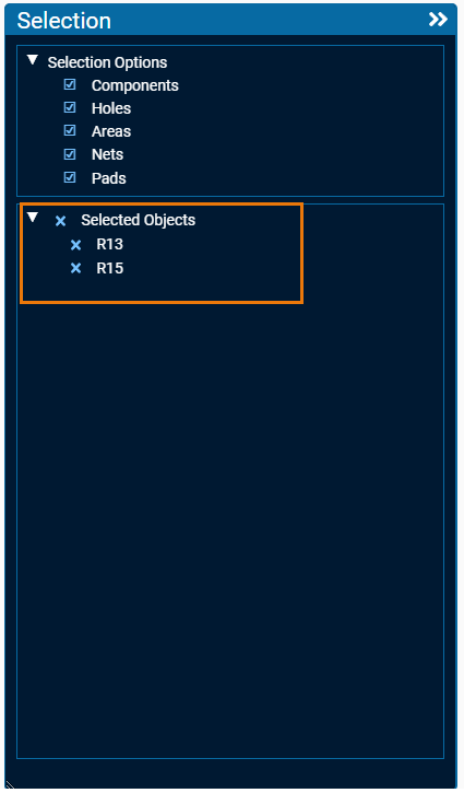
On the viewer command ribbon, click Selection Toolbox
 to
open the Selection toolbox.

Notice the two selected components listed in the Selected Objects group.
-
On the viewer command ribbon, click Overlays Toolbox
 to open the
Overlays toolbox where you can specify additional
data, such as component reference designators.
Note:To expand the graphics view in the main window, you can collapse any toolbox by clicking
 to collapse it.
 - In the Component Data group, from the component data list, select Bottom.
- Clear the Pins check box to only display the reference designators.
-
Use the component data search box,to filter the list of displayed reference designators, and select the check boxes for desired designators to display them.
If you do not know the reference designator, you can refer to the interactive table on the Components tab to easily find it.

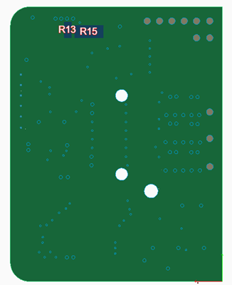
The software superimposes the reference designator labels on the model with a colored outline. You can modify the colors of the label and its outline using the viewer preferences on the Settings page.
-
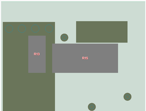
On the viewer command ribbon, click Focus Camera View on Current
Selection
 to zoom into
the area surrounding the selected PCB entities.
The software automatically adjusts the opacity of the model to highlight the selection.
-
On the viewer command ribbon, click Measurement Mode
 to enable the
measurement feature that lets you measure the spacing between PCB entities and
attributes in millimeters.
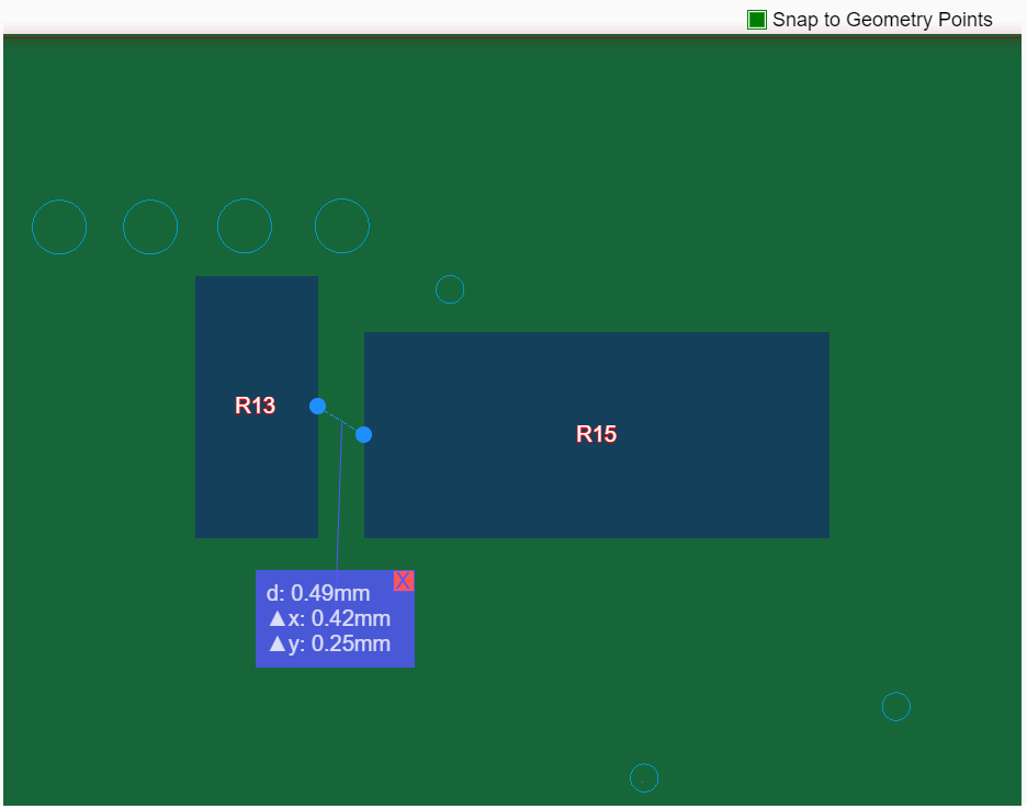
- In the graphics window, select the Snap to Geometry Points check box.
-
Select two points on the edge of the PCB entity to display the shortest
distance values between the points. For example, select the polygon edge of one
component, and the nearest edge of the second component.

In the example shown, the distance between the two points is 0.49mm, the distance in the X direction is 0.42mm and in the Y direction is 0.25mm. You can verify if this meets the required design manufacturing rules.
-
To capture an image of the displayed model, from the viewer command ribbon,
click Export View to PNG
 and save the
PNG file to your desired location.
